The following image shows the browser presentation.
 |
| Chrome with AdcHttpd on a BeagleBone Black with 16 bit DDC data from a LX9 |
The main area is a HTML5 canvas which is drawn using a basic graphing toolkit I developed for instrumentation purposes. The buttons at the bottom are HTML buttons with javascript actions. The first row allows presentation changes (envelope, peak picking, user markers, storing a memory, changing Y limits). The second row controls server side parameters such as the function to perform, in this case PSE or power spectral estimation, the number of points to produce, the number of averages to use, the channel to select and the LO frequency used in down conversion. The channel is the tap point referenced in the DDC. The final row sets the state to run or not run, or resets various pieces of software. The line above the graph also includes key parameters in effect along with the date and status of the connection to the http server (it turns red and indicates not connected if a threshold of failed server requests is reached).
The numeric quantities that are free form input (e.g. F1(Hz) or LO mixer or the upper and lower graph limits) are entered via a javascript keypad. The following screen capture shows the same channel or signal as the previous capture but this time in the time domain and with the keypad popped up to modify the Y limits.
 |
| Javascript Keypad Input (Time series in background of signal in previous figure) |
The browser tab consumes about 10% of a CPU core on an older PC (AMD 1.8GHz quad core) and about 1% load on the Ethernet interface. The BeagleBone is at 98% running the http server. The BBB limits the update rate based on its ability to process the samples (fftw for ARM is used for best performance).
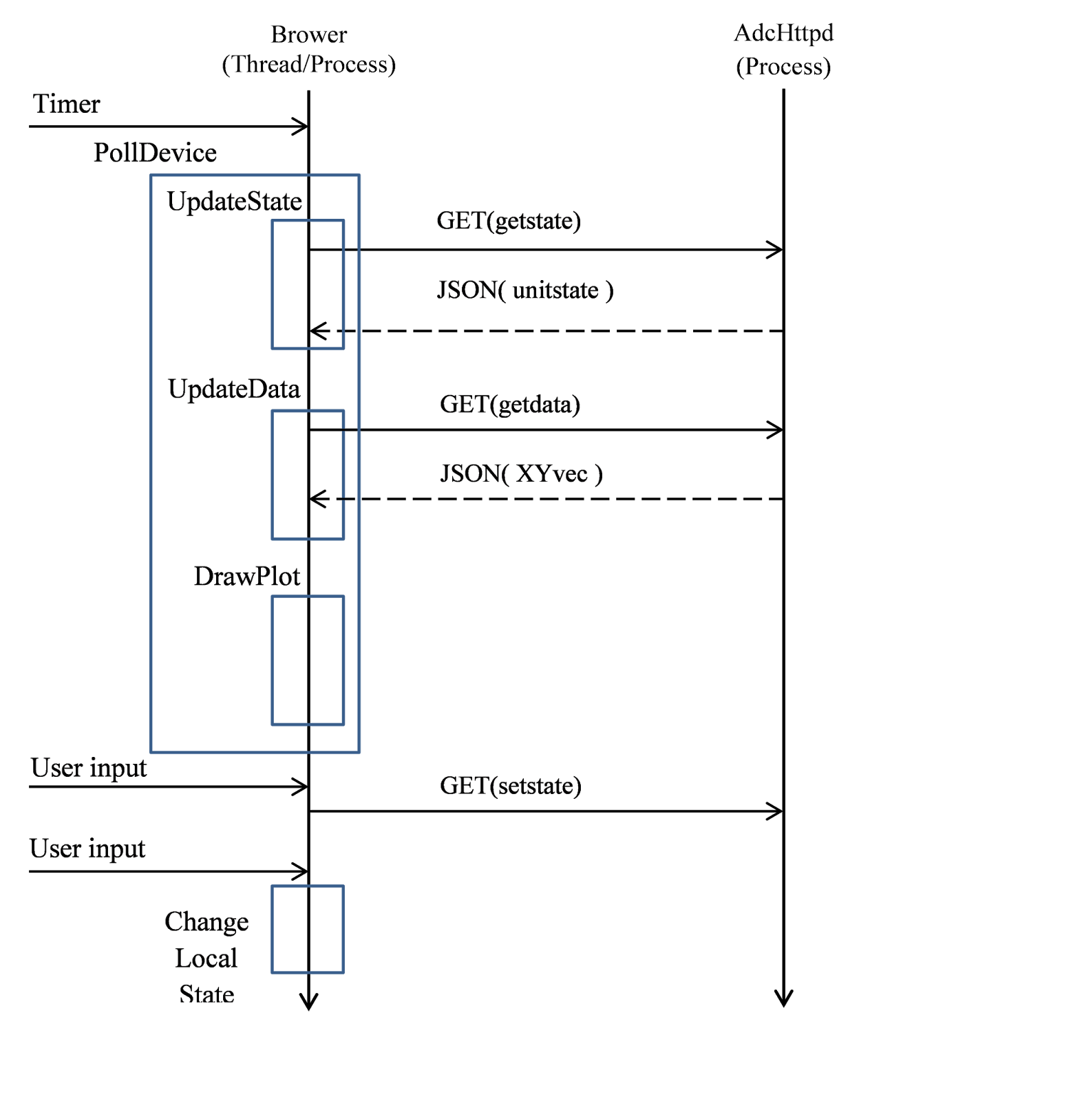
There are several components to the internals of the browser code, http server code, hardware model, and device code on the BeagleBone Black. The basic model is that the server is the definitive controller of state and operations while the browser code simply requests changes and conducts presentation. At the highest level the following sequence diagram summarizes the interactions of the application.
 |
| Browser-AdcHttpd Summary Sequence Diagram |
The Browser lifeline captures the javascript code behavior executing within the browser while the AdcHttpd lifeline captures the software executing on the BeagleBone Black. There are only two events handled by the javascript code: a timer and user input. The timer forces a sequence of events which boil down to getting state and data from the server and drawing a plot of the current data. All information is obtained from the server via http GET requests. The results coming from the server are JSON text representing application variables. The diagram is slightly off in that the responses coming back are processed asynchronously to the request. There is additional logic to keep the state requests at a lower request rate than the requests for data. In addition, there is logic to adjust the polling rate based upon the operational state of the instrument. Quantities in the overall state include things like channel number to process, run/stop state, mixer frequency. The data coming from the server is just a x,y list of points to be plotted on the graph.
The other events processed by the browser javascript are user inputs. This ends up taking two forms: a) those which change server state and are sent directly to the server, and b) those which change local browser application state and can be processed without interaction with the server. Examples of the former include run/stop state or channel number and examples of the later include graphing x and y limits, peak picking enable/disable, and markers on/off.
The server is more involved and is responsible for not only acquiring the data and processing it but also presenting it in JSON format to the client. The following sequence diagram summarizes the key server components and interactions.
 |
| Summary Sequence Diagram of AdcHttpd Internals |
There are only two autonomous lifelines here by design. The first is the http server thread that interacts directly with the client and processes the http GET requests. The second is the hardware model thread which drives processing of data and hardware interactions. The only point the two threads interact is the hardware data model. The interactions are designed to require minimal locking and interaction between the two autonomous threads. This keeps things conceptually simple and decouples the browser client and its interactions and requests from the core hardware servicing and operations. The hardware object model contains the current and desired operation parameters along with the most recent XY data to be presented in the browser application.
The hardware model thread checks various operating parameters based on their current value in the memory shared with the http thread. If changes have occurred, the hardware model thread calls the appropriate device object methods to change the operating parameters. Examples include which channel is being processed/exported by the hardware and the frequency of the downconversion local oscillator. After a check on current parameters the hardware model thread invokes the ProcessCoherentInterval() on one of the processing objects. There are processing objects for each of the main types of processing: power spectral estimation, time series, and histogram. The product of processing a coherent interval is a set of XY points which is updated in the hardware model (and can then be accessed by the remote client via the main http thread). The hardware model thread continually loops on this processing until a reset is conducted.
Each of the processing objects deals with a coherent interval a little differently. The key one is the power spectral estimation processing. Since the data rates of the selected ADC channel can exceed the processing capability (indeed the network transport capacity), a processing interval is treated as a flush of current ADC data followed by the acquisition of one or more sets of 2k samples. The collected data is treated as a coherent set and in the case of spectral estimation has a window applied along with an FFT and magnitude and normalization applied to produce the XY results. In the case of low sample rate channels, 16k or more samples can be treated coherently since successive Get2k calls retrieves contiguously sampled data. For streams with high bandwidth, the user simply has to not configure power spectra estimates greater than 2k (if you do you just get phase discontinuities across 2k sample sets and see spectrum broadening).
The device object encapsulates different boards. There are a common set of C++ ADC and Mixer interfaces required that each board exports. The startup method for the device object selects which boards and interfacing software to use. This can be done by configuration file, code changes or reasoning on which device tree(s) are currently installed.